01
Introduction to Analog circuit and Layout design
Basics of analog circuit design concepts, Analog circuit design challenges and implementation strategies, Introduction to Analog layout concepts, Layout design rules and process
02
IC Fabrication flow
Introduction to fabrication techniques, Ionization and wafer technology, CMOS/BJT/MOSFET/FINFET IC fabrication steps, Fabrication techniques for Deep submicron technology
03
Introduction to Analog layout concepts
Understanding various mask layers, Layout requirements for each layers, Layout floor planning, BUMP/PAD/ESD/PIN planning
04
Introduction to Layout editor tools
Creating libraries, adding and managing layout cell views, Creating config views for DRC/LVS checks, Layout editor tool commands and shortcuts, Commands for creating netlist from schematics and exporting to layout view, Layout spice simulation commands
05
Standard Cell Layout design
Layout of basic CMOS gates, INV, AND, NAND, OR, NOR, Complex cell layout design
06
Layout or Discrete components
BJT, DIODE, Clamp cell designs, Resister, Capacitors, Inductors design, BiCMOS logic designs
07
Layout Design Techniques
Orientations, Multifingers/common Centriod/Quads, Distance/Gaps between layout layers, Overlaying and Adjacent layers, Same Area/Perimeter ratios, soft edge shapes
08
Layout Design Checks
DRC/ERC/LVS soft checks, Electro migration checks and Removal techniques, IR Drop analysis, Antenna affect checks and Removal techniques, SI checks like crosstalk and EMI issues, ESD checks and ESD cell designs, Dish effects checks and removal, Well proximity checks
09
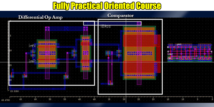
Analog Layout Designs
Analog Amaplifiers, comparators, filters circuits, Opamp sense amplifier designs, Differential Opamp Designs, Bandgap layout Designs, BUMP/ESD/Gaurd ring designs, Tap Cell Designs
10
Memory Layout Designs
SRAM cell design, Rows and Columns Decoders, Sense Amplifier design, Write/read control logic, Power supply design, Dual port RAM cell designs
11
Final Project
1. PLL, LDO, ADC layouts. In 65nm, 32nm, 14nm
2. Assignments given for Lab practice


QuestVLSI Technologies is one of the best training institute for VLSI Analog Layout Design, teaching faculty having working industry professional and teaches very well.
Ashish Gupta
November 10, 2019